
Silicon is widely used as a semiconductor material due to its abundance in nature. But researchers around the world are actively trying to find superior alternatives, and diamonds are among the most promising materials for applications in high-power electronics. Diamond has semiconductor properties superior to those of silicon carbide (SiC), silicon (Si), and gallium nitride (GaN), such as high thermal conductivity, insulation, and a wide bandgap.
Despite its superior attractive properties for the semiconductor industry, diamond is still not considered a reference material for power electronic devices because of its very high mechanical hardness and smaller size of substrates. The hardness of a diamond makes it challenging to slice a thick diamond crystal into thin wafers efficiently. Because of this, diamond wafers must be synthesized one by one, making fabrication costs prohibitive for most industries.
To resolve this, researchers from Chiba University developed a novel laser-based technique for effortlessly slicing diamonds along the optimal crystallographic plane, thus producing smooth wafers.
Laser slicing is a technique of slicing materials along cracks formed by scanning a focused ultrashort-pulse laser beam inside the materials.
The properties of most crystals carry along different crystallographic planes – imaginary surfaces containing the atoms comprising the crystal. A diamond can be easily sliced along the {111} surface, but slicing {100} is challenging because it also produces cracks along the {111} cleavage plane, increasing kerf loss.
To control the formation of these undesirable cracks through the diamond, researchers developed a diamond processing technique that focuses short laser pulses onto a narrow cone-like volume within the material.
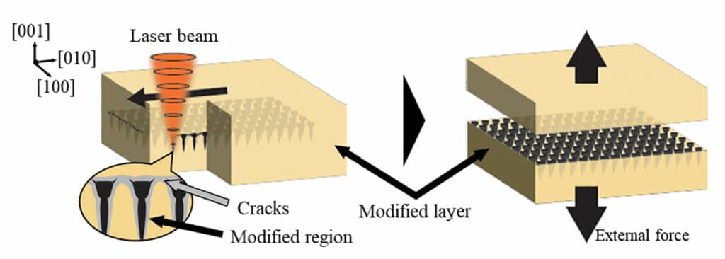
“Concentrated laser illumination transforms diamond into amorphous carbon, whose density is lower than that of diamond. Hence, regions modified by laser pulses undergo a reduction in density and crack formation,” lead researcher Hirofumi Hidai explained.
The researchers used the laser pulses to create a grid-like pattern of small crack-prone regions inside the material. These regions help guide the propagation of cracks along the desired plane. As a result, a smooth wafer with {100} surface can be easily separated from the rest of the block by simply pushing a sharp tungsten needle against the side of the sample.
Overall, this slicing technology could potentially pave the way toward making diamonds a suitable semiconductor material for future technologies.
“Diamond slicing enables the production of high-quality wafers at low cost and is indispensable to fabricate diamond semiconductor devices. Therefore, this research brings us closer to realizing diamond semiconductors for various applications in our society, such as improving the power conversion ratio in electric vehicles and trains,” Professor Hidai said in the press release.
Journal reference:
- Kosuke Sakamoto, Daijiro Tokunaga, Sho Itoh, Hirofumi Hidai, Souta Matsusaka, Takashige Omatsu, Koji Koyama, Seong-Woo Kim, and Noboru Morita. Laser slicing of a diamond at the {100} plane using an irradiation sequence that restricts crack propagation along the {111} plane. Diamond & Related Materials, 2023; DOI: 10.1016/j.diamond.2023.110045