
Graphene is a one-atom-thick layer of carbon atoms arranged in a hexagonal lattice. It is the most excellent material ever discovered. Almost 200 times stronger than steel, lighter than paper, graphene is the most robust material ever.
Now, Korean scientists have successfully grown and characterized single-crystal graphene with no wrinkles, folds, or adlayers- the most perfect graphene to date.
Factors behind this discovery include human ingenuity and the ability to reproduce make large-area single-crystal Cu-Ni(111) foils. The graphene was grown by chemical vapor deposition (CVD) using ethylene with hydrogen in a stream of argon gas.
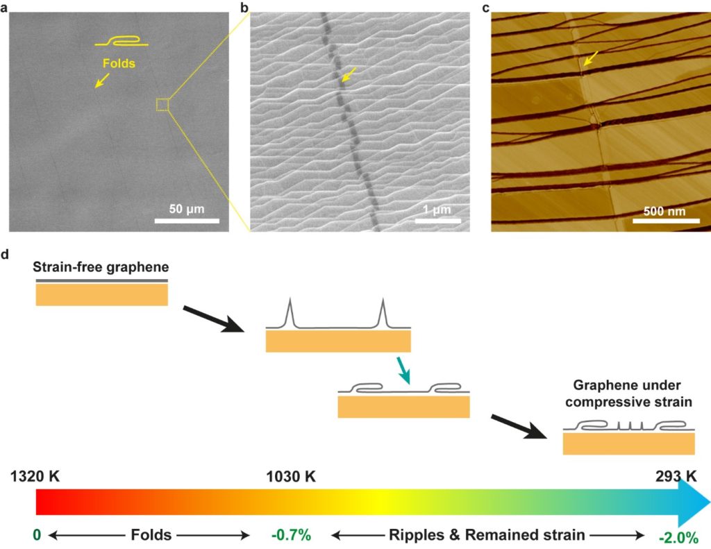
Scientists experimented with growing single-layer and single-crystal graphene on homemade’ Cu-Ni(111) foils under different temperatures. They started with implementing a series of ‘cycling’ experiments that involved ‘cycling’ the temperature immediately after growing the graphene at 1320 K. Through these experiments, scientists showed that the folds in graphene structure are formed at or above 1020 K during the cooling process.
A team of scientists conducted the research, led by Director Rodney Ruoff at the Center for Multidimensional Carbon Materials (CMCM) within the Institute for Basic Science (IBS), including graduate students at UNIST.
After knowing this, scientists grow graphene on Cu-Ni(111) foils at several different temperatures around 1020 K. This leads to a discovery that large-area, high-quality, fold-free, and adlayer-free single-crystal graphene films can be grown in a temperature range between 1000 K and 1030 K.
Won Kyung Seong, a senior research fellow in CMCM who installed the LEED equipment in the center, said, “This fold-free graphene film forms as a single crystal over the entire growth substrate because it shows a single orientation over a large-area low-energy electron diffraction (LEED) patterns.”
Scientists then patterned GFETs on this single-crystal fold-free graphene in several directions. These GFETs showed remarkably uniform performance with average room temperature electron and hole mobilities of 7.0 ± 1.0 × 103 cm2 V-1 s-1. Such remarkably uniform performance is possible because the fold-free graphene film is a single crystal with essentially no imperfections.
Student Meihui Wang at UNIST said, “Importantly, we were able to achieve “scaling up” of graphene production using this method. The graphene was successfully grown simultaneously on five foils (dimension 4 cm x 7 cm) in a 6-inch diameter home-built quartz furnace. Our method of growing fold-free graphene films is very reproducible, with each foil yielding two identical pieces of high-quality graphene films on both sides of the foil,” and “By using the electrochemical bubbling transfer method, graphene can be delaminated in about 1 minute. The Cu-Ni(111) foil can be quickly readied for the next growth/transfer cycle.”
“When we tested the weight loss of Cu-Ni(111) foils after five runs of growth and transfers, the net loss was only 0.0001 grams. This means that our growth and transfer methods using the Cu-Ni(111) can be performed repeatedly, essentially indefinitely.”
While achieving this fold-free, most perfect graphene, scientists also discovered the reason behind the folds. They performed high-resolution TEM imaging to observe the cross-sections of the samples grown above 1040 K. They discovered that the deadhesion, which is the cause of the folds, is initiated at the “bunched step edge” regions between the single crystal Cu-Ni(111) plateaus.
Co-corresponding author Luo said, “This deadhesion at the bunched step edge regions triggers the formation of graphene folds perpendicular to the step edge direction. We discovered that step-bunching of a Cu-Ni(111) foil surface suddenly occurs at about 1030 K, and this ‘surface reconstruction’ is the reason why the critical growth temperature of fold-free graphene is at ~1030 K or below.”
Such large-area fold-free single-crystal graphene film allows for the straightforward fabrication of high-performance integrated devices oriented in any direction over the entire graphene film. These single-crystal graphene films will be important for further advances in basic science, which will lead to new applications in electronic, photonic, mechanical, thermal, and other areas.
Journal Reference:
- Wang, M., Huang, M., Luo, D. et al. Single-crystal, large-area, fold-free monolayer graphene. Nature 596, 519–524 (2021). DOI: 10.1038/s41586-021-03753-3