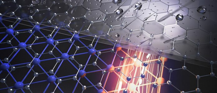
Finding substitute materials that retain their functionality at the atomic level is one of science’s most significant difficulties as silicon-based computer processors approach their physical limits to pursue faster and smaller designs.
In an innovative discovery, scientists from the Würzburg-Dresden Cluster of Excellence ct. qmat has created a barrier that protects quantum semiconductor layers that are only one atom thick from outside effects without sacrificing their ground-breaking quantum characteristics. This makes using exceedingly thin atomic layers in fragile electrical components feasible.
In 2021, scientists made a breakthrough discovery: topological quantum materials like indenene, which have enormous potential for ultrafast, energy-efficient electronics. The resulting ultrathin quantum semiconductors function as topological insulators, conducting electricity almost without resistance along their edges. They are made up of a single atom layer, in this case, indium atoms in the case of indecent.
Experimental physicist Professor Ralph Claessen, ct. qmat’s Würzburg spokesperson said, “Producing such a single atomic layer requires sophisticated vacuum equipment and a specific substrate material. To utilize this two-dimensional material in electronic components, it must be removed from the vacuum environment. However, exposure to air, even briefly, leads to oxidation, destroying its revolutionary properties and rendering it useless.”
Cedric Schmitt, one of Claessen’s doctoral students involved in the project, said, “We dedicated two years to finding a method to protect the sensitive indenene layer from environmental elements using a protective coating. The challenge was ensuring that this coating did not interact with the indenene layer.”
“This interaction is problematic because when different types of atoms – from the protective layer and the semiconductor, for instance – meet, they react chemically at the atomic level, changing the material. This isn’t a problem with conventional silicon chips comprising multiple atomic layers, leaving sufficient layers unaffected and still functional.”
Ralph Claessen said, “A semiconductor material consisting of a single atomic layer such as indenene would normally be compromised by a protective film. This posed a seemingly insurmountable challenge that piqued our research curiosity. The search for a viable protective layer led them to explore van der Waals materials, named after the Dutch physicist Johannes Diderik van der Waals.”
“These two-dimensional van der Waals atomic layers are characterized by strong internal bonds between their atoms while only weakly bonding to the substrate. This concept is akin to how pencil lead is made of graphite – a form of carbon with atoms arranged in honeycomb layers – and writes on paper. The layers of graphene can be easily separated. We aimed to replicate this characteristic.”
The Würzburg team investigated the conditions required to create graphene from silicon carbide (SiC) by heating it as a substrate for indenene using advanced ultrahigh vacuum equipment. Atoms of silicon and carbon make up silicon carbide. The carbon atoms separate from the surface when heated, forming graphene.
Schmitt elucidates the laboratory process: “We then vapor-deposited indium atoms, which are immersed between the protective graphene layer and the silicon carbide substrate. This is how the protective layer for our two-dimensional quantum material indenene was formed.”
Without sacrificing the remarkable quantum features of a two-dimensional quantum semiconductor material, scientists successfully created a functioning protective layer for the material for the first time in history. They examined the manufacturing procedure in detail and then tested the layer’s resistance to corrosion and oxidation.
“It functions! Claessen exclaims, “The sample can even be submerged in water without experiencing any negative effects. Our indenene is protected by the graphene layer like an umbrella.”
This innovation makes applications requiring extremely sensitive semiconductor atomic layers possible. Ultrathin electrical components must be treated in air or other chemical conditions throughout their manufacturing. The identification of this defense mechanism has made this feasible.
The Würzburg team is now focusing on finding more van der Waals materials that can act as protective layers, and they are already considering a few options. The problem is that short circuits can occur due to graphene’s electrical conductivity, even if it shields atomic monolayers from outside influences. Overcoming these obstacles and laying the groundwork for tomorrow’s atomic layer electronics are the goals of the Würzburg scientists.
Journal Reference:
- Achieving environmental stability in an atomically thin quantum spin Hall insulator via graphene intercalation device. Cedric Schmitt, Jonas Erhardt, Philipp Eck, Matthias Schmitt, Kyungchan Lee, Philipp Keßler, Tim Wagner, Merit Spring, Bing Liu, Stefan Enzner, Martin Kamp, Vedran Jovic, Chris Jozwiak, Aaron Bostwick, Eli Rotenberg, Timur Kim, Cephise Cacho, Tien-Lin Lee, Giorgio Sangiovanni, Simon Moser, Ralph Claessen in Nat Commun 15, 1486 (2024). DOI: 10.1038/s41467-024-45816-9.
