Scientists from the Center for Multidimensional Carbon Materials (CMCM), within the Institute for Basic Science (IBS) at UNIST, have fabricated single crystal copper-nickel alloy foil substrates for the growth of large-area, single-crystal bilayer and trilayer graphene films. This new work is expected to provide materials for the fabrication of graphene devices with novel functions that have not yet been realized.
This study demonstrated the first example of the synthesis of bi-and trilayer graphene sheets more significant than a centimeter, with layers accumulated in a particular way, to be namely AB-and ABA-stacking.
Distinguished Professor Ruoff, the leading author of this study, said, “This work provides materials for the fabrication of graphene devices with novel functions that have not yet been realized and might afford new photonic and optoelectronic and other properties. This paves the way for the study of novel electrical transport properties of the bilayer and trilayer graphene.”
Coauthor Pavel V. Bakharev notes that: “Less than one year ago, we produced fluorinated diamond monolayer, F-diamane, by fluorination of exactly the AB-stacked bilayer graphene films described in this new paper. Now the possibility of producing bilayer graphene of a larger size brings renewed excitement and shows how fast this field is developing.”
Selecting the right substrate is essential for the correct growth of graphene. Copper made foils limit the growth of bilayer graphene and favor uniform monolayer growth. Obtaining multilayer graphene sheets on nickel film is possible but, these are not uniform and tend to have small “patches” with different thicknesses. Finally, the commercially available foils that contain both nickel and copper are not ideal.
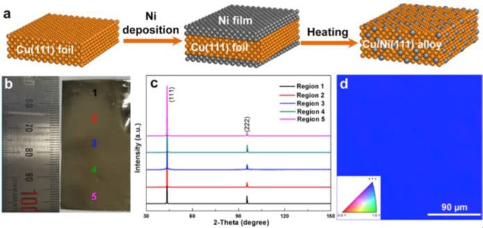
Thus, IBS scientists prepared ‘home-made’ single crystal Cu/Ni(111) foils with desired features, assembling further on a technique detailed by the group in Science in 2018. Nickel films are electroplated onto copper(111)- thwarts with the goal that the nickel and copper interdiffusion when heated and yield a new single crystal foil that contains both elements at adjustable ratios. This strategy and Ming Huang’s evolutions of the best concentrations of nickel to acquire uniform graphene sheets with the desired number of layers.
Scientists were able to grow bi- and tri-layer graphene sheets on Cu/Ni(111) foils by chemical vapor deposition (CVD). Scientists achieved AB-stacked bilayer graphene films of several square centimeters, covering 95% of the substrate area, and ABA-stacked trilayer graphene with more than 60% areal coverage. This represents the first growth of high coverage ABA-stacked trilayer graphene over a large city and the best quality obtained for AB-stacked bilayer graphene so far.
Scientists also measured the electrical transport (carrier mobility and bandgap tunability) and thermal conductivity of the newly synthesized graphene. The centimeter-scale bilayer graphene films showed an excellent thermal conductivity, as high as ~2300 W/mK (comparable with exfoliated bilayer graphene flakes), and mechanical performance (stiffness of 478 gigapascals for Young’s modulus, and 3.31 gigapascals for the fracture strength).
Ming Huang said, “We showed with three independent methods that the 2nd layer for bilayer graphene, and the 2nd and 3rd layers of the trilayer sheet grow beneath a continuous top layer. These methods can be further used to study the structure and stacking sequence of other 2D thin-film materials.”
Distinguished Professor Rodney S. Ruoff (School of Natural Science) from the Center for Multidimensional Carbon Materials (CMCM) said, “these techniques for synthesizing and testing large-scale ultrathin films could stimulate worldwide interest in further experimenting with single crystal Cu/Ni alloy foils, and even in exploring fabrication and use of other single-crystal alloy foils.”
The work has been published in Nature Nanotechnology on January 21, 2020.
