
An international team of scientists from the Center for Multidimensional Carbon Materials (CMCM), within the Institute for Basic Science (IBS) at UNIST, has recently created a single layer (adlayer-free) graphene film on large area copper foils. This may appear the most recent in a progression of apparently comparable affirmations on single-layer graphene, but this accomplishment varies from many previous publications as none of them had depicted really single-layer graphene over a large area.
Scientists refined the chemical vapor deposition (CVD) growth method by killing all carbon contaminant inside the copper foils on which graphene is developed. CVD on metal foils (particularly copper foils) is presently the most encouraging way for adaptable and reproducible synthesis of large-area films movies of high quality. The group explored why “adlayers” showed up in the graphene film developed on copper foils and found that the carbon contaminants within the foil directly lead to the nucleation and growth of adlayers.
Dr. Da Luo, first author of the article said, “We discovered that the commercial copper foils have ‘excess carbon’ particularly near the surface—to a depth of about 300 nm, by using time-of-flight secondary ion mass spectrometry and combustion analysis. From a discussion with one technical expert in Jiangxi Copper Corporation Limited, one of the world’s largest suppliers of copper foils, we learned that the carbon is embedded in the copper foil during manufacture, probably from hydrocarbon-based oil(s) used to lubricate rollers that the copper foil contacts at the high rolling temperatures. After completely removing this carbon by annealing under H2 at 1060 °C, they were able to achieve adlayer-free and thus truly single-layer graphene film.”
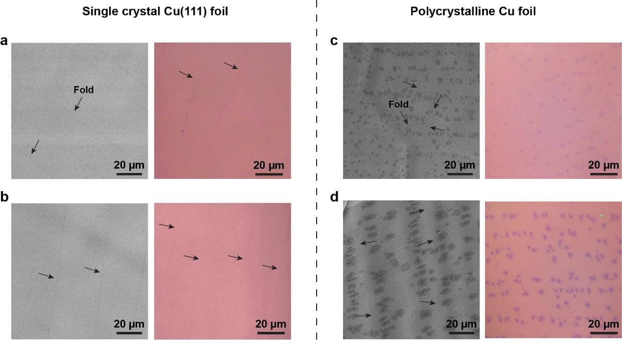
IBS scientists also applied the same process and obtained adlayer-free single layer and single crystal graphene film on a single crystal Cu foil.
One of the first authors Meihui Wang explained, “We thus solved two problems that have persistently been present in prior syntheses of CVD graphene films (adlayers and grain boundaries (GBs)) at one time.”
In fact, achieving ideal consistency in the number of layers over a large area zone (single or twofold layers, for instance) can be utilized to ensure a consistent device performance.
Adlayer regions differ in, e.g., density and size when present in the active regions of devices. Along with adlayers, GBs are available in polycrystalline graphene films arranged by CVD where graphene islands with various crystallographic orientations join to complete the film. The presence of GBs brings down bearer portability and thermal conductivity and diminishes the mechanical strength.
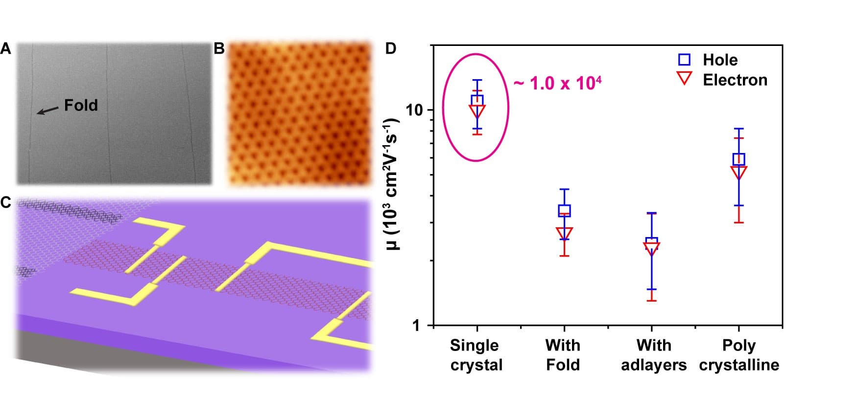
Still, the scientists were left with one fascinating feature in their single crystal films: This single crystal graphene contains highly oriented parallel “folds” that are centimeters in length, roughly a hundred nanometers in width, and separated by 20 to 50 micrometers. Just like adlayers and GBs, folds were observed to significantly decrease the carrier mobility of graphene.
To dispose of such dispersing effects of adlayers, GBs, and folds, scientists designed field-effect transistors in the region lying between two adjoining folds and with the transistors parallel to the folds. Unlike folds distributed quasi-randomly in the polycrystalline graphene film, the folds are profoundly adjusted in the enormous region single crystal graphene film. This makes it simple to create high-performance devices from the areas between the folds.
Wang said, “The region between two adjacent folds is ‘clean’ without any folds, adlayers, or GBs. This enabled the device to have a very high electron and hole mobility. The field-effect transistors show very high room temperature carrier mobility values of around 1.0 x 104 cm2V-1s-1. Such high carrier mobility “translates” to various useful devices having high performance.”
Rodney S. Ruoff, Distinguished Professor, School of Natural Sciences, UNIST said, “Our approach towards large area adlayer-free single-crystal graphene is a breakthrough. This uniform, ‘perfect’ single layer, single crystal graphene is expected to find use as an ultrathin support material for high-resolution transmission electron microscopy imaging, and in optical devices. Also as appropriate graphene to achieve extremely uniform functionalization which leads to many other applications, particularly for sensors of various types. I also would like to note that we greatly valued the strong contributions by coauthors from UNIST, from HKUST, and from SKKU.”
The study is published in the journal Advanced Materials.