
Graphene and other two-dimensional (2D) materials hold great promise for creating electronic and optoelectronic devices due to their unique properties. However, the challenge of transferring them effectively over large areas has hindered their widespread use.
A new study by Kyushu University, in collaboration with Japanese company Nitto Denko, report a transfer method that uses functional tapes with adhesive forces controlled by ultraviolet light. Scientists have devised a new adhesive tape that can be used to stick 2D materials to many different surfaces easily and user-friendly.
The researchers initially concentrated on graphene, composed of a single layer of carbon atoms arranged in a two-dimensional lattice. One of the primary techniques for producing graphene is chemical vapor deposition, in which graphene is synthesized on a copper film. However, graphene needs to be separated from the copper substrate and transferred onto an insulating surface such as silicon for optimal performance.
Lead author Professor Hiroki Ago of Kyushu University’s Global Innovation Center said, “To do this, a protective polymer is placed over the graphene, and the copper is then removed using an etching solution, such as acid. Once attached to the new substrate, the protective polymer layer is dissolved with a solvent. This process is costly, time-consuming, and can cause defects to the graphene’s surface or leave traces of the polymer behind.”
In this study, researchers aimed to offer an alternative way of transferring graphene. They used AI to develop a specialized polymer tape, dubbed “UV tape,” which changes its attraction to graphene when irradiated with UV light.
Before exposure to UV light, the tape forms a strong bond with graphene, firmly attaching to it. However, once exposed to UV light, the atomic bonding in the tape alters, reducing its adhesion to graphene by approximately 10%. Additionally, the UV-treated tape becomes slightly stiffer and more manageable to peel off. These combined changes enable the video to be removed from the device substrate while leaving the graphene intact.
Additionally, the researchers created tapes capable of transferring two other 2D materials: hexagonal boron nitride (hBN), also known as white graphene, which serves as an insulator and protective layer when stacking 2D materials, and transition metal dichalcogenides (TMDs), a promising material for future semiconductors.
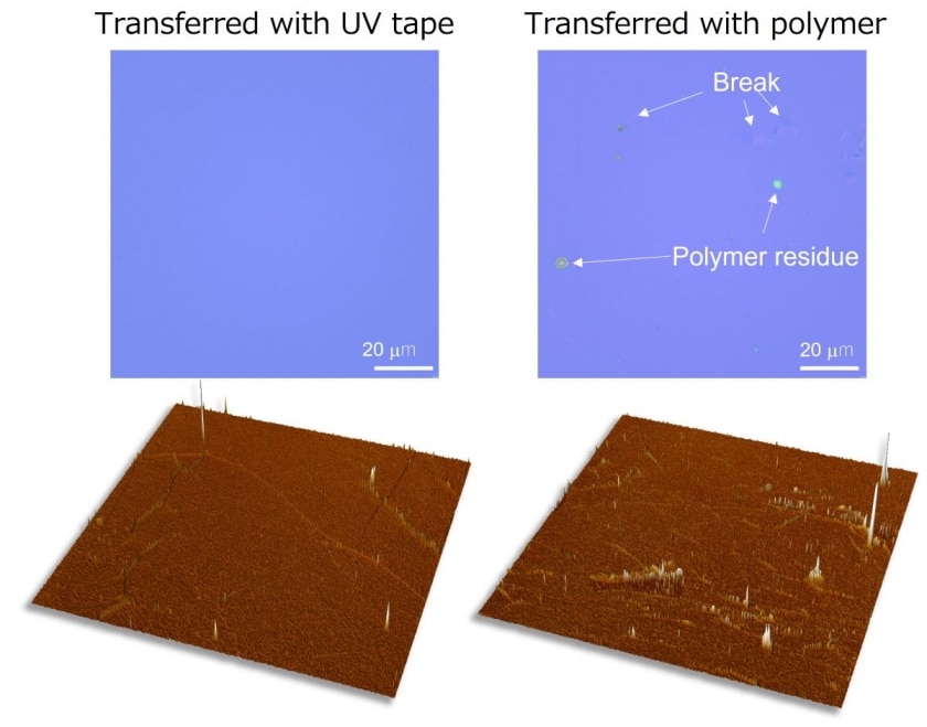
Upon closely examining the surfaces of the transferred 2D materials, the researchers observed smoother surfaces with fewer defects than those transferred using conventional methods. Furthermore, testing revealed that these materials exhibited enhanced efficiency in their properties.
Furthermore, utilizing UV tape for transfer presents several other benefits compared to existing techniques. The flexibility of the UV tape allows for the use of flexible plastics as the substrate for the device, eliminating the need for plastic-dissolving solvents during the transfer process. This feature expands the range of potential applications for these devices, particularly in areas requiring flexibility.
Professor Ago says, “For example, we made a plastic device that uses graphene as a terahertz sensor. Like X-rays, terahertz radiation can pass through objects that light can’t, but doesn’t damage the body. It’s very promising for medical imaging or airport security.”
The UV tape can also be precisely cut to the required size, ensuring that only the necessary amount of 2D material is transferred. This not only minimizes waste but also reduces costs. Moreover, researchers can easily stack layers of different 2D materials on top of each other in various orientations, allowing them to explore novel properties arising from combining these materials.
In their future endeavors, the researchers aim to scale up the production of UV tape to meet the needs of manufacturers. Currently, the largest graphene wafer that can be transferred using this method is 10 cm in diameter. The team is also working to address issues such as wrinkles and bubbles that may form on the tape, leading to small defects.
Furthermore, they are focused on enhancing the stability of the UV tape, enabling 2D materials to remain attached for longer periods, thus facilitating distribution to end-users such as other scientists.
Professor Ago said, “The end users can then transfer the material onto their desired substrate by applying and removing the UV tape like a child’s sticker, with no training needed. Such an easy method could fundamentally change the style of research and accelerate the commercial development of 2D materials.”
Journal Reference:
- Maki Nakatani, Satoru Fukamachi, Pablo Solís-Fernández et al. Ready-to-transfer two-dimensional materials using tunable adhesive force tapes. Nature Electronics, DOI: 10.1038/s41928-024-01121-3