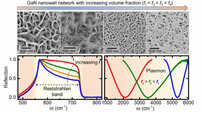
Gallium nitride (GaN), a widely used material for blue light emission, is one of the most advanced semiconductors– useful for light-emitting diodes, power electronics, and optoelectronic applications. Extending GaN’s optical resonance from visible to mid- and far-infrared spectral ranges will enable novel applications in many emerging technologies.
GaN nanostructures can be used to restrict and absorb IR light, creating extremely effective IR absorbers, emitters, and modulators for imaging, sensing, energy production, and other applications.
Infrared light emission and absorption with GaN nanostructures have been shown for the first time by scientists at the Jawaharlal Nehru Centre for Advanced Scientific Research (JNCASR), an independent institute of the Department of Science and Technology in Bengaluru.
This is the first time infrared light-matter interactions in GaN have been observed, despite the fact that blue light emission from GaN has long been known and is employed in LEDs. For this demonstration, they have used a scientific phenomenon known as surface polariton excitations in GaN nanostructures, which result in light-matter interactions in the IR spectral range.
Surface polaritons are particular electromagnetic wave modes when a conductor and an insulator, like air, come into contact. They can also induce plasmon polaritons in GaN by modifying the morphology and form of the nanostructures, which extends the light-matter interaction to further portions of the electromagnetic spectrum. These polaritons are quasi-particles with properties similar to both light and matter.
The scientists used a sophisticated material deposition tool called molecular beam epitaxy in the International Centre for Materials Science in JNCASR to create these GaN nanostructures. This device grows high-quality material nanostructures with dimensions around 100000 times smaller than the width of a human hair using ultra-high vacuum, which is equivalent to the conditions in space.
The development of polariton-based electronics, which have various advantages over traditional electronic devices, is made possible by such cutting-edge materials. Applications for polaritonic technology include:
- Quantum computers.
- Waste-heat converters.
- Next-generation light sources.
- Solar energy converters.
- Secure high-speed light-based communication (LiFi).
Dr. Bivas Saha, Assistant Professor at the Jawaharlal Nehru Centre for Advanced Scientific Research, said, “In the last 25 years, blue LED with GaN has changed our world significantly. While the blue light emission from GaN is well-understood, utilizing GaN for infrared optics is not well-established. Our work demonstrates a novel pathway for utilizing GaN in infrared nanophotonic applications. Importantly, the scientists said that the infrared surface polariton excitations we have demonstrated can be translated to many other semiconductors as well.”
“This work will greatly benefit in addressing the demand for IR sources and detectors for energy, security, imaging, and other applications.”
Journal Reference:
- Krishma Chand Maurya, Abhijit Chatterjee, Sonnada Math Shivaprasad, and Bisvas Saha. Morphology-Controlled Reststrahlen Band and Infrared Plasmon Polariton in GaN Nanostructures. Nano Letters. DOI: 10.1021/acs.nanolett.2c03748
