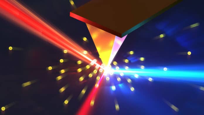
Electrons distribution and dynamics in semiconductor materials often govern their physical properties, critical to functionalities and performance in industrial applications. The continued miniaturization of electronic and photonic devices calls for tools to probe carrier behavior in semiconductors simultaneously at the picosecond time and nanometer length scales.
UC Berkeley researchers have now demonstrated a new type of optical nanoscopy that can measure electron dynamics in semiconductors. They developed a pump–probe optical nanoscopy integrated with near-field scanning optical microscopy and pump-probe optics to enable high resolution at both spatial and temporal scales.
Furthermore, this approach applies to a broad variety of semiconductor materials, such as silicon, germanium, and gallium arsenide, as well as other uncommon materials, including 2D materials and ferroelectrics.
Optical nanoscopy uses ultrafast lasers and an atomic force microscope (AFM) tip with an apex curvature of less than 30 nanometers to monitor semiconductors’ electrons. Researchers shine the AFM tip with two laser beams: a pump beam and a probe beam.
After a precisely timed delay, the second beam impacts the tip after the first beam has excited the sample’s electrons. The analysis of the second beam’s scattered light can then be used to determine the local information on electron characteristics.
Jingang Li, lead author and a postdoctoral researcher in Grigoropoulos’s Laser Thermal Lab, said, “Optical nanoscopy may have applications beyond measuring electrons in semiconductor materials.”
“Because it’s a versatile optical diagnostic tool, it can study many other physical phenomena and functional devices, such as phase transitions and data storage.”
“This research represents an important step toward investigating and optimizing energy savings for semiconductor-based electronic devices — such as mobile phones, LEDs, industrial solar cells, and sensors.”
Journal Reference:
- Jingang Li, Rundi Yang, Yoonsoo Rho* et al. Ultrafast Optical Nanoscopy of Carrier Dynamics in Silicon Nanowires. Nano Letters. DOI: 10.1021/acs.nanolett.2c04790
