
Two-dimensional (2D) materials, which are only one atom thick, resemble nanosized building blocks that can be stacked arbitrarily to frame little gadgets. At the point when the lattices of two 2D materials are comparative and well-aligned, a repeating pattern called a moiré superlattice can form.
Since the last decade, scientists are studying various ways to combine different 2D materials, often starting with graphene. Out of this body of work, other researchers had discovered that moiré superlattices formed with graphene exhibit exotic physics such as superconductivity when the layers are aligned at just the right angle.
In a new study by the Department of Energy’s Lawrence Berkeley National Laboratory (Berkeley Lab), scientists have developed an easier way to transform ordinary semicondcuting materials into quantum machines. Such development could potentially revolutionize a number of industries aiming for energy-efficient electronic systems – and provide a platform for exotic new physics.
The study demonstrates the way that stacks 2D layers of tungsten disulfide together with tungsten diselenide to create an intricately patterned material or superlattice.
For this study, scientists used 2D samples of semiconducting materials – tungsten disulfide and tungsten diselenide – to show that the twist angle between layers provides a “tuning knob” to turn a 2D semiconducting system into an exotic quantum material with highly interacting electrons.
Feng Wang, a condensed matter physicist with Berkeley Lab’s Materials Sciences Division and professor of physics at UC Berkeley said, “This is an amazing discovery because we didn’t think of these semiconducting materials as strongly interacting. Now this work has brought these seemingly ordinary semiconductors into the quantum materials space.”
Scientists fabricated the tungsten disulfide and tungsten diselenide samples using a polymer-based technique to pick up and transfer flakes of the materials, each measuring just tens of microns in diameter, into a stack.
They then quantified the optical absorption of a new tungsten disulfide and tungsten diselenide sample and found that the absorption of visible light in a tungsten disulfide/tungsten diselenide device is largest when the light has the same energy as the system’s exciton, a quasiparticle that consists of an electron bound to a hole that is common in 2D semiconductors. (In physics, a hole is a currently vacant state that an electron could occupy.)
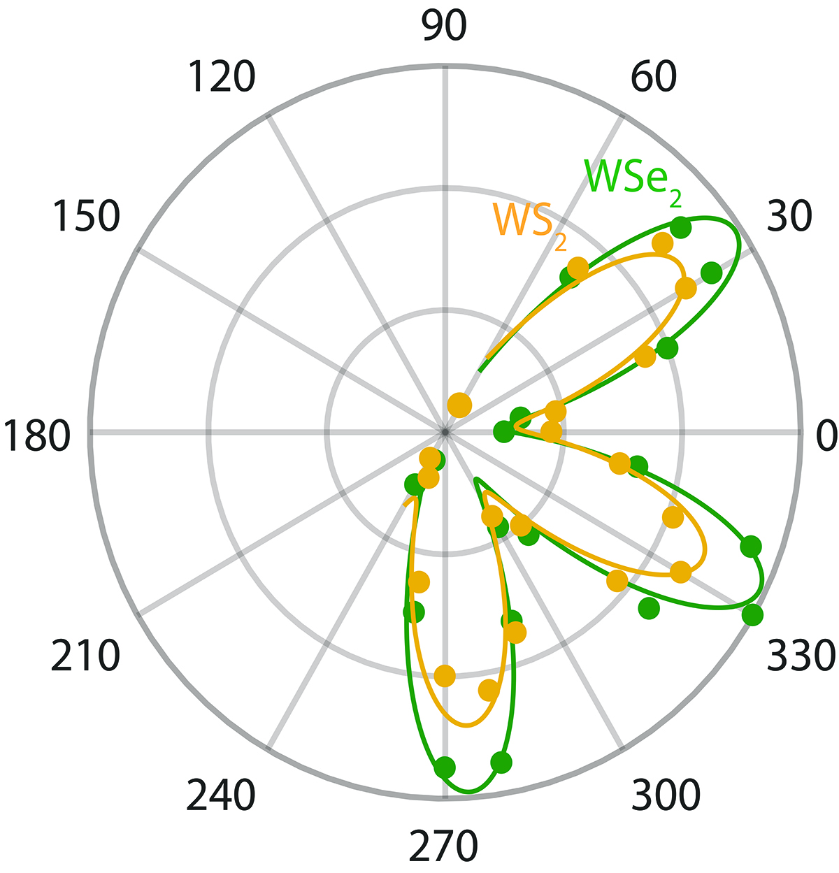
For light in the energy range that the researchers were considering, they expected to see one peak in the signal that corresponded to the energy of an exciton.
Instead, they found that the original peak that they expected to see had split into three different peaks representing three distinct exciton states.
What could have increased the number of exciton states in the tungsten disulfide/tungsten diselenide device from one to three? Was it the addition of a moiré superlattice?
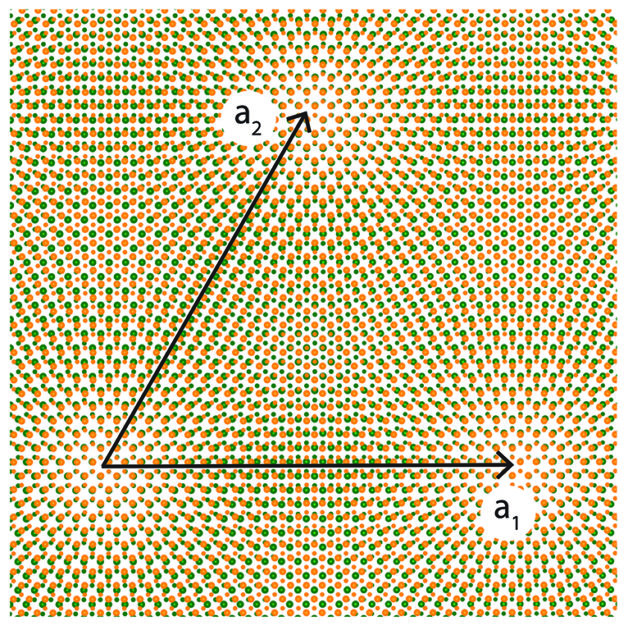
To find out, scientists used a transmission electron microscope (TEM) at Berkeley Lab’s Molecular Foundry, a nanoscale science research facility, to take atomic-resolution images of the tungsten disulfide/tungsten diselenide device to check how the materials’ lattices were aligned.
Emma Regan, a graduate student researcher who work under Wang in the Ultrafast Nano-Optics Group at UC Berkeley said, “The TEM images confirmed what we had suspected all along: the materials had indeed formed a moiré superlattice. We saw beautiful, repeating patterns over the entire sample. After comparing this experimental observation with a theoretical model, we found that the moiré pattern introduces large potential energy periodically over the device and could, therefore, introduce exotic quantum phenomena.”
Scientists are now planning to measure how this new quantum system could be applied to optoelectronics, which relates to the use of light in electronics; valleytronics, a field that could extend the limits of Moore’s law by miniaturizing electronic components; and superconductivity, which would allow electrons to flow in devices with virtually no resistance.
The study was conducted in the collaboration with Arizona State University and the National Institute for Materials Science in Japan.
The study was published online recently in the journal Nature. The work was supported by the DOE Office of Science. Additional funding was provided by the National Science Foundation, the Department of Defense, and the Elemental Strategy Initiative conducted by MEXT, Japan, and JSPS KAKENHI. The Molecular Foundry is a DOE Office of Science user facility.