Semiconductor micro-LEDs are appealing for display technologies due to their great optical contrast, brightness, energy efficiency, and long operational lifetimes. Because of their fast switching speeds and compatibility with CMOS drive circuits, these devices are quickly expanding in research and industrial domains, including spatially modulated imaging, optical wireless communications, wearable/implantable optoelectronic displays, and biomedical sensor systems.
Researchers developed a continuous roller printing technology that accurately transfers over 75,000 micrometer-scale semiconductor devices in a single roll. This approach paves the path for large-scale optical component arrays and could be used to build micro-LED screens quickly.

Micro-LED display technology is appealing because it can achieve highly accurate color rendering with high speed and resolution while requiring little power. These displays can be used in various applications, such as smartphones, virtual and augmented reality devices, and enormous displays several meters across. The obstacles of integrating millions of small LEDs onto an electrical control backplane are considerable for more extensive micro-LED displays.
According to a Researcher at the University of Strathclyde in the United Kingdom, the roller-based printing technique offers a scalable way to achieve this while meeting the high accuracy required for this application. Research team leader Eleni Margariti from the University of Strathclyde in the UK said, “Transferring micrometer-scale semiconductor devices from their native substrate to a variety of receiving platforms is a challenge being tackled internationally by academic research groups and industries.”
The roller technology can match the planned device layout with an accuracy of less than 1 micron. The setup is also low-cost and simple enough to be built in areas with limited resources.
This printing technology could also be utilized for various devices, such as transistors, sensors, and antennas for flexible and wearable electronics, innovative packaging, and radio-frequency identification tags. It could also create photovoltaics and healthcare applications such as drug delivery systems, biosensors, and tissue engineering.
Researchers aimed to increase the performance and scaling of electronic systems used in applications such as displays and on-chip photonics by improving the transfer of huge semiconductor devices from one substrate to another. The new method begins with a collection of tiny devices loosely linked to their development substrate.
A cylinder with a slightly sticky silicone polymer film on its surface is then rolled over the suspended array of devices, allowing adhesive forces between the silicone and semiconductors to separate the devices from their growing substrate and array them on the cylinder drum.
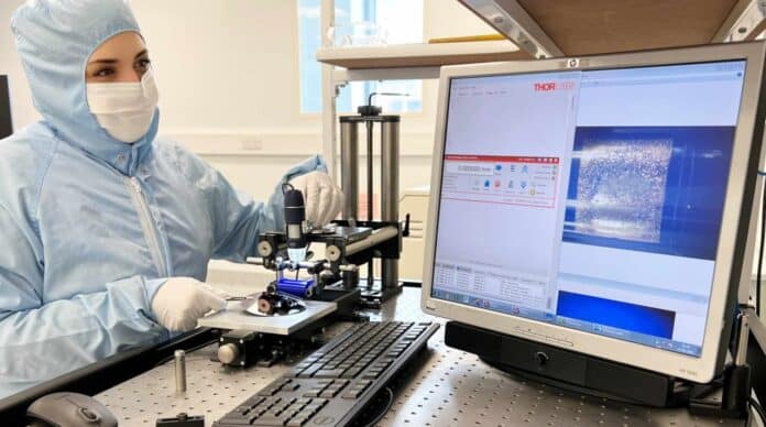
The printing yield and positioning accuracy are provided in minutes by carefully selecting the properties of the silicone and receiving substrate surface, the speed and mechanics of the rolling process, and the custom analysis method that scans the printed sample for defects and provides the printing yield and positioning accuracy in minutes.
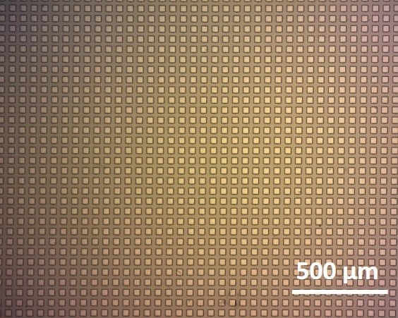
The researchers used gallium nitride on silicon (GaN/Si) semiconductor structures to test the novel technique, the leading semiconductor technology used for micro-LED displays. They could transmit more than 99% of the devices in a 76,000-element array with less than a micron spatial precision and no significant rotational errors.
The researchers are trying to increase the printing process’s precision while increasing the number of devices that may be transferred simultaneously. They intend to put the technology to the test in terms of its capacity to mix different types of devices on the same receiving platform and to see if it can be used to print to specified spots on the receiving platform.
Journal Reference:
- E. Margariti, G. Quinn, D. Jevtics, et al. Continuous roller transfer-printing and automated metrology of >75,000 micro-LED pixels in a single shot. Optical Material Express.DOI: 10.1364/OME.483657
