
If it were possible to observe the movements of atoms and electrons within materials in real-time, many scientific and technical challenges could be quickly addressed. Scientists have sought to comprehend their remarkable optical properties in the realm of halide perovskites, a mineral class widely utilized in technologies from solar cells to quantum applications.
A team led by Nuri Yazdani, Vanessa Wood at ETH Zurich, and Aaron Lindenberg at Stanford, along with colleagues at Empa in Dübendorf, has made notable advancements, studying atom motion within nanocrystals with a time resolution in the range of billionths of a second.
Scientists took snapshots of the crystal structure of perovskite nanocrystals as excited electrons deformed it. To their surprise, the deformation straightened out the skewed crystal structure rather than making it more disordered.
Yazdani said, “Halide perovskites are great for many optoelectronic applications. But it is puzzling how this class of materials can exhibit such outstanding optical and electronic properties.”
“We have known that when perovskites absorb light, excited electrons to higher energies couple strongly to phonons inside the material. Often, one can treat the average position of each atom inside a crystal as fixed, but that is no longer possible when an optical excitation of an electron leads to a large reorganization of the crystal lattice.”
Scientists were wondering: how do excited electrons in perovskites change the shape of the crystal lattice?
Scientists in this study peer inside a perovskite (formamidinium lead bromide) synthesized at Empa using an ultrafast electron diffraction beamline facility at the SLAC. The facility emits very short pulses of electrons that last only a hundred femtoseconds, or a millionth of a second.
After striking the roughly 10-nanometer-sized perovskite nanocrystals, these electrons diffract, and the electrons are gathered on a screen. Due to their quantum nature, electrons behave like waves. As a result, when they diffract from the atoms within the material, the electron waves may interfere constructively or destructively, depending on the atoms’ positions and the direction of diffraction. This is analogous to light passing through two slits. This method allows for measuring even minute changes in the crystal structure.
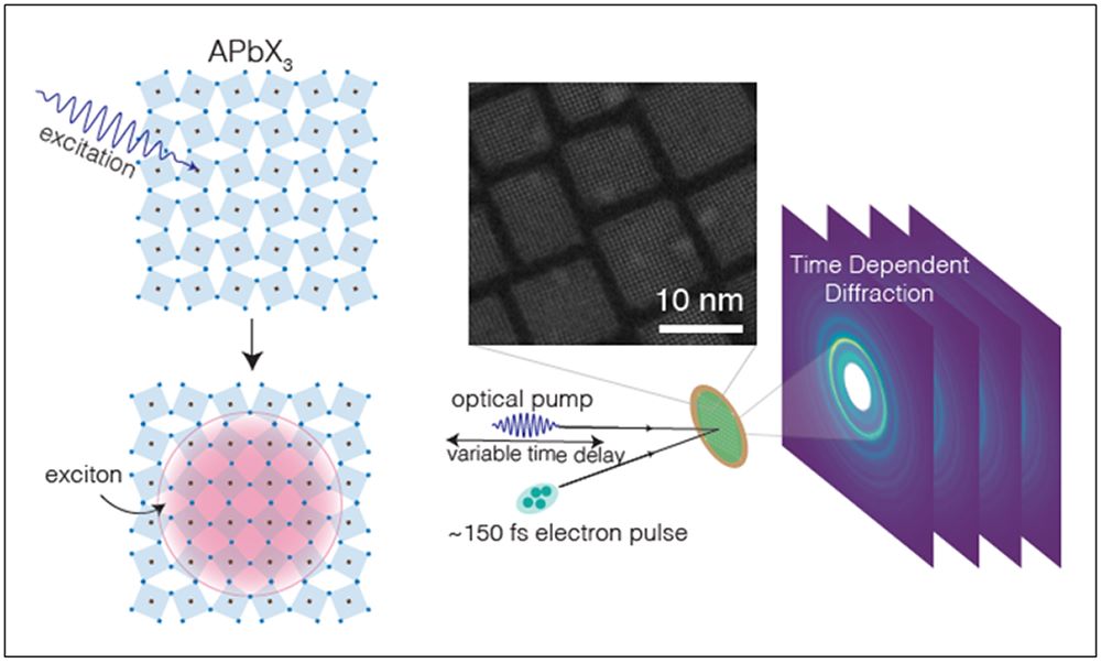
Utilizing a unique capability of the SLAC beamline, the ETH researchers captured images of the crystal structure before and after photon absorption. Employing a laser for photon generation and electron pulse initiation allowed precise control of photon arrival time relative to electrons by adjusting the travel distance. Analyzing these snapshots over several hundred picoseconds revealed the temporal evolution of the crystal lattice deformation induced by photo-excited electrons.
The results surprised scientists. Instead of seeing crystal deformation causing symmetry reduction, they observed a shift towards increased symmetry – the excited electrons had slightly straightened out the skewed crystal structure of the perovskite.
The model calculations suggested that several excitons – bound pairs of excited electrons and positively charged holes left behind by their excitation – could cooperate in straightening the lattice. Since that lowers their total energy, the excitons were effectively attracted to one another.
Yazdani said, “Understanding the origin of the electron-phonon coupling will make it easier to produce perovskites with particular optical properties tailor-made for specific applications.”
“For instance, perovskite nanocrystals for next-generation T.V. screens can be coated in a shell of another material to reduce the electron-phonon coupling and hence reduce the spectral linewidth of the emitted light. This was already demonstrated in 2022.”
“Also, since the attractive interaction between excitons is similar to the mechanism that allows electrical current to flow without loss in superconductors, that attraction might be exploited to enhance electron transport. This could, in turn, be useful for making solar cells based on perovskites.”
Journal Reference:
- Yazdani, N., Bodnarchuk, M.I., Bertolotti, F., Kovalenko, M.V., Wood, V., Lindenberg, A.L. et al. Coupling to octahedral tilts in halide perovskite nanocrystals induces phonon-mediated attractive interactions between excitons. Nat. Phys. (2023). DOI: 10.1038/s41567-023-02253-7