
Thermoelectric (TE) materials are popular because they enable energy conversion between heat and electricity. Those devices are made from materials that can convert a temperature difference into electricity, without requiring any moving parts. This quality makes thermoelectrics a potentially appealing source of electricity.
Now a team of scientists at UNIST has introduced a new class of thermoelectric materials with superior performance and efficiency. For their work, they have attracted so much attention from the scientific community by convert that otherwise wasted heat into electricity, using their own thermoelectric technique.
Scientists have successfully fabricated highly aligned SnSe thin films through a low-cost and scalable solution process. Their process is originally a two-step process, which involves dissolving SnSe powder in a solvent composed of ethylenediamine and ethanedithiol, and purifying the resulting solution with acetonitrile to obtain a precipitate.
Seung Hwae Heo in the Combined M.S/Ph.D. of Materials Science and Engineering at UNIST said, “Compared with polycrystalline SnSe, which has a unique layered crystal structure like a stack of paper, SnSe thin films exhibit TE power factors at the single crystal level. As wrinkles in papers lower the quality of the prints, polycrystalline materials also lower thermoelectric efficiencies.”
In order to construct high-performance TE devices, superior TE materials have to be targeted via various strategies. In particular, the single crystal SnSe owing to its unexpectedly low thermal conductivity and high power factor. However, their efficiencies are limited, due to the challenges associated with controlling the crystal structure of SnSe.
Scientists solved this process by developing a two-step solution process to grow SnSe in a particular direction. The process involves dissolving SnSe powder in a solvent composed of ethylenediamine and ethanedithiol, and purifying the resulting solution with acetonitrile to obtain a precipitate to fabricate highly textured SnSe thin films.
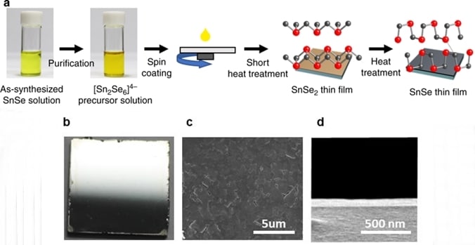
The precipitate was dissolved in ethylenediamine to obtain the SnSe ink solution. The ink was spin-coated on a glass substrate and the film was heated for 1 min at 400℃. The coating process was repeated to obtain the desired thickness. Finally, the film was annealed at 400℃ for an appropriate time.
Seungki Jo in the Combined M.S/Ph.D. of Materials Science and Engineering at UNIST said, “Upon heating, Se evaporation occurs, which then leads to the transition from SnSe2 to SnSe in the thin film. It seems that the previously formed SnSe is serving as a milestone, allowing the newly-formed SnSe crystal structures to be aligned.”
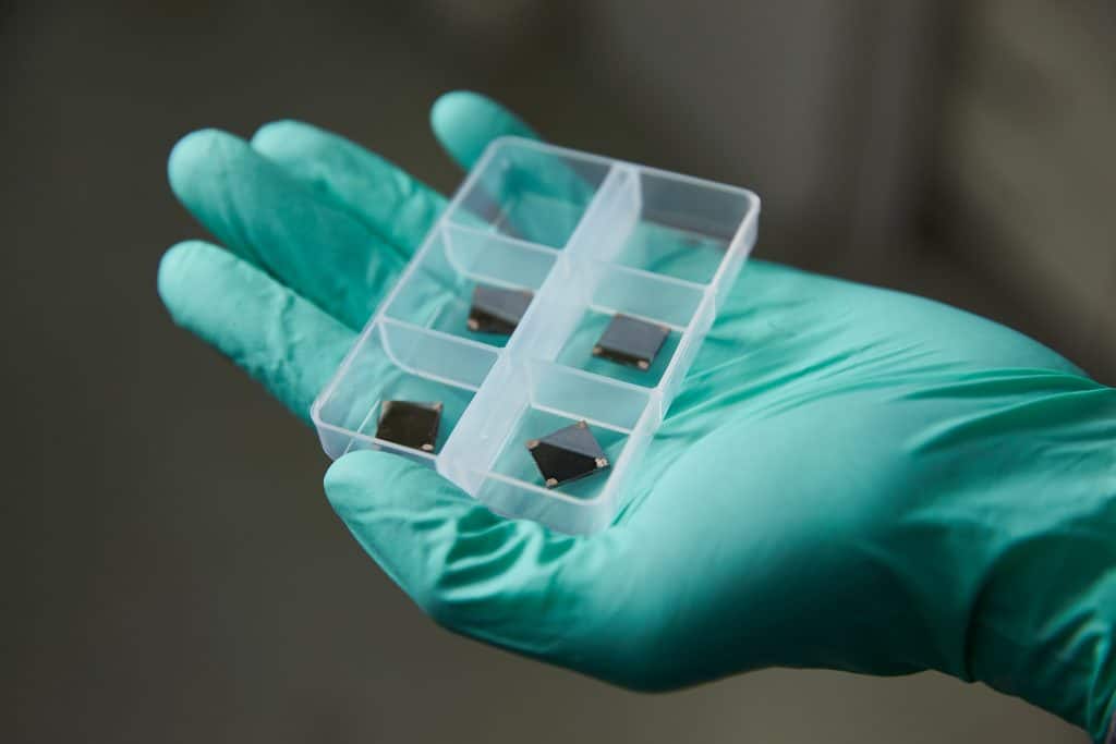
The new SnSe thin film exhibit 10 times higher electrical properties than the previous study. In addition, it showed high performance comparable to that of a lump of SnSe material.
The examination group additionally discovered that it is easy to improve the physical properties by controlling the structure of the completed slight film material. This is on the grounds that the proportion of selenium molecules shaping precious stones can be adaptably balanced by altering the warmth treatment temperature and time. In this investigation, tin-selenide films were likewise heat-treated at 400℃ for 1 minute, 5 minutes, 9 minutes, and 13 minutes, separately.
Professor Son said, “This new technology is not only simple and efficient but also controls the direction of tin- selenide crystals. With the technology, we can now manufacture high-performance thermoelectric thin films at low cost, and it will help develop standards for the measurement of ultra-thin film thermoelectric materials.”