
In quantum materials, photocurrent is frequently gathered at global contacts, far from the initial photoexcitation. The process of collection is rather nonlocal. In addition to the arrangement of the current collecting contacts, the spatial nonuniformity and tensor conductivity structure and the complicated spatial pattern of photocurrent flow (streamlines) away from its initial photoexcitation all play essential roles in this process. It isn’t easy to track photocurrent streamlines directly with imaging.
A new study at the University of California, Riverside, demonstrates a microscopy method to image photocurrent streamlines through ultrathin heterostructure devices. The study showed how electrons flow around sharp bends, such as those found in integrated circuits, has the potential to improve how these circuits, commonly used in electronic and optoelectronic devices, are designed.
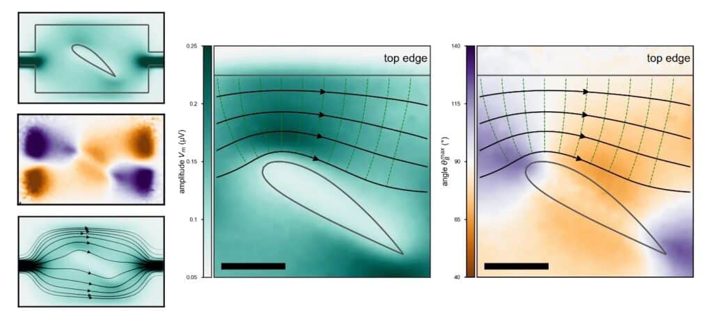
Scientists designed an electrofoil- a new device- to image streamlines of electric current. Electrofoil is a new type of device that allows for the contortion, compression, and expansion of streamlines of electric currents in the same way airplane wings contort, compress, and expand the flow of air.
Nathaniel M. Gabor at the University of California said, “The team combined laser imaging with novel light-sensitive devices to develop the first images of photocurrent streamlines through a working device. A photocurrent is an electric current induced by the action of light.”
“If you know how the electrons are flowing, you can then know how to prevent them from causing harmful effects, such as heating the circuit. With our technique, you can now assess exactly where and how the electrons flow, giving us a powerful tool to visualize, characterize, and measure charge flow in optoelectronic devices.”
Electrons heat up after gaining kinetic energy. Ultimately, they heat the material around them, such as wires that can risk melting. That’s what happens with electronic devices when they heat up.
Scientists designed the electrofoils as little wing shapes in nanoscale devices that make the electrons flow around them, similar to how air molecules flow around an airplane wing.
Gabor said, “We wanted a shape that could give us different turning rates, something with a continuous curvature. We took inspiration from airplane wings, which have a gradual curve. We forced the current to flow around the electrofoil, which offers different angles of flight. The sharper the angle, the more the compression of the flow lines. We are starting to find that electrons behave like liquids in more and more materials. So rather than design devices based on electrical resistance, we can adopt an approach with plumbing in mind and design pipelines for electrons to flow through.”
Scientists used a microscopy method that uses a uniform rotating magnetic field to image photocurrent streamlines through ultrathin devices made of a layer of platinum on yttrium iron garnet, or YIG. YIG is an insulator but allows for a magnetic field effect when a thin layer of platinum is glued to it.
Gabor said, “The magnetic field effect shows up only at the interface of this garnet crystal and platinum. If you can control the magnetic field, you control the current.”
The scientists focused a laser beam on YIG, using the laser as a local heat source to create a photocurrent in the desired direction. The “photo-Nernst effect” produces the photocurrent, whose direction is determined by the external magnetic field.
Gabor said, “Direct imaging to track photocurrent streamlines in quantum optoelectronic devices remains a key challenge in understanding exotic device behavior. Our experiments show that photocurrent streamline microscopy is a robust new experimental tool to visualize a photocurrent in quantum materials. This tool helps us look at how electrons misbehave.”
Electrons act in “weird ways” under certain circumstances, notably in tiny devices.
Gabor said, “Our technique can now be used to study them better. If I were trying to design an integrated circuit and wanted to know where heat might originate in it, I would want to know where the current flow lines are being squeezed. Our technique can help design circuits, estimate what to avoid, and suggest you should not have sharp bends in your wires. Wires should be gradually curved. But that is not the state of the art right now.”
Journal Reference:
- David Mayes, Farima Farahmand et al. Mapping the intrinsic photocurrent streamlines through micromagnetic heterostructure devices. PNAS. DOI: 10.1073/pnas.2221815120