Scientists from the U.S. Department of Energy’s Lawrence Berkeley National Laboratory (Berkeley Lab), have developed a new way to assemble transistors and circuits that are only a few atoms thick. With functional structures, this new method has applications in the real world and commercial scalability. Integration of this technique with other developing systems may cause future computing will be done completely with atomically thin crystals.
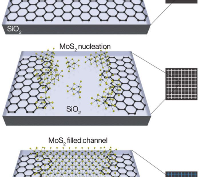
Scientists controlled the combination of the transistor. In the transistor, confined channels were etched upon conducting graphene and blank channels are filled with transition-metal dichalcogenide (TMDC). All this thin material are single-layered crystals. Therefore, the two-part assembly brings electronic structures that are necessarily two-dimensional. Additionally, this combination also covers the little area.
Xiang Zhang, a senior scientist in Berkeley Lab’s Materials Sciences Division who led the study, said, “This is a scalable and repeatable way to develop atomically thin electronics or pack more computing power into a smaller area.”
With the intention of keeping a new step with Moore’s Law, that consists of the number of transistors in an integrated circuit. To do this, scientists expressed integrated electronics will require transistors. The transistor must be of less than ten nanometers in length in size.
Silicon is heavy material. Therefore, using silicon transistor in nanometre scale is not a good choice. Equipment made from silicon become smaller and smaller and their performance decreases dramatically. Thus, it may become a major barrier for future electronics. Scientists took one thick molecule with two-dimensional crystals as substitute materials to maintain with Moore’s Law. These tiny crystals aren’t exposed to the silicon force.
Discovery behind this atomically thin transistors and circuits
In this tone, scientists’ have cultivated a new way to develop a single-layered semiconductor. The TMDC molybdenum disulphide (MoS2) was used to fill channels upon conducting graphene sheet. The two atomic sheets combine to form nanometre-scale junctions. This allows graphene to effectively insert current into the MoS2. These junctions create atomically thin transistors.
Mervin Zhao, a Ph.D. student in Zhang’s group at Berkeley Lab and UC Berkeley, said, “This approach allows for the chemical assembly of electronic circuits, using two-dimensional materials, which show improved performance compared to using traditional metals to inject current into TMDCs.”
Different features related to the successful formation and functionality of the two-dimensional transistors is confirmed by Optical and electron microscopy images, and spectroscopic mapping.
Additionally, the scientists also found the relevance of the structure by assembling it into the logic circuitry of an inverter. According to scientists, “This highlights technology abilities to lay the foundation for a chemically assembled atomic computer.”
Zhao said, “Both of these two-dimensional crystals have been combined in the wafer scale in a way that is compatible with current semiconductor manufacturing. By integrating our technique with other growth systems, it’s possible that future computing can be done completely with atomically thin crystals.”
