
Bridging the “terahertz gap “relies upon synthesizing arbitrary waveforms in the terahertz domain enabling applications that require both narrow band sources for sensing and few-cycle drives for classical and quantum objects. However, a realization of custom-tailored waveforms needed for these applications needs to be improved due to limited flexibility for optical rectification of femtosecond pulses in bulk crystals.
Researchers at EPFL‘s School of Engineering’s Laboratory of Hybrid Photonics (HYLAB), under the direction of Cristina Benea-Chelmus, have made significant progress toward effectively utilizing the so-called terahertz gap, which lies between roughly 300 and 30,000 gigahertz (0.3 and 30 THz) on the electromagnetic spectrum. This frequency range, which describes frequencies that are too fast for modern electronics and telecommunications equipment yet too slow for optical and imaging applications, is currently considered a technical dead zone.
The HYLAB researchers and their associates at ETH Zurich and Harvard University have now achieved not only the production of terahertz waves but also the engineering of a method for specifically customizing their frequency, wavelength, amplitude, and phase. This was made possible by a fragile chip with an integrated photonic circuit constructed of lithium niobate. Terahertz radiation can now potentially be used for next-generation applications in both the electrical and optical fields thanks to such fine control over it.
Co-first author Alexa Herter, currently a Ph.D. student at ETH Zurich, said, “Seeing the devices emit radiation with properties that we predefined was a confirmation that our model was correct.”
Co-first author Amirhassan Shams-Ansari, a postdoctoral fellow at Harvard University, said, “This was made possible due to the unique features of lithium niobate integrated photonics.”
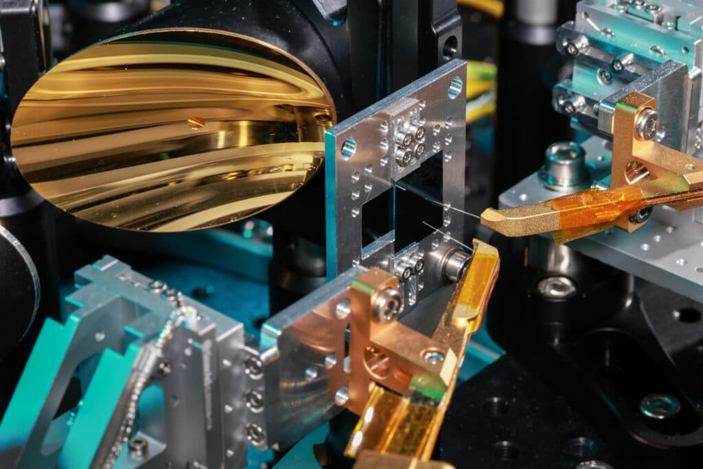
Benea-Chelmus said, “While such terahertz waves have been produced in a lab setting, previous approaches have relied primarily on bulk crystals to generate the right frequencies. Her lab’s use of the lithium niobate circuit, finely etched at the nanometer scale by collaborators at Harvard University, makes their novel approach much more streamlined. Using a silicon substrate makes the device suitable for integrating into electronic and optical systems.”
“Generating waves at very high frequencies is extremely challenging, and very few techniques can generate them with unique patterns. We can now engineer the exact temporal shape of terahertz waves – to say essentially, ‘I want a waveform that looks like this.”
To do this, Benea-Chelmus’ group created the chip’s configuration of waveguides, or channels, from which minuscule antennas broadcast terahertz waves produced by light from optical fibers.
Benea-Chelmus said, “The fact that our device already uses a standard optical signal is an advantage because it means that these new chips can be used with traditional lasers, which work very well and are well understood. It means our device is telecommunications-compatible.”
“Miniaturized devices that send and receive signals in the terahertz range could play a key role in sixth generation mobile systems (6G).”
Benea-Chelmus believes that tiny lithium niobate chips have special promise for spectroscopy and imaging in optics. Terahertz waves are non-ionizing and have a lot lower energy than many other types of waves (like x-rays) that are now employed to reveal the chemical makeup of a substance, whether it is an oil painting or a bone. Therefore, a less intrusive substitute for the current spectrographic methods could be offered by a small, non-destructive device like the lithium niobate chip.
Benea-Chelmus said, “You could imagine sending terahertz radiation through a material you are interested in and analyzing it to measure the material’s response, depending on its molecular structure. All this from a device smaller than a match head.”
Researchers are further planning to tweak the properties of the chip’s waveguides and antennas to engineer waveforms with greater amplitudes and more finely tuned frequencies and decay rates. They also expect that their terahertz technology could be useful for quantum applications.
Journal Reference:
- Herter, A., Shams-Ansari, A., Settembrini, F.F. et al. Terahertz waveform synthesis in integrated thin-film lithium niobate platform. Nat Commun 14, 11 (2023). DOI: 10.1038/s41467-022-35517-6