
Ultrathin materials are increasingly replacing traditional thick glass lenses used today in cameras and imaging systems. These engineered lenses — known as metalenses, consist of materials constructed at the nanoscale into arrays of columns or fin-like structures.
Now, scientists at the University of Washington and the National Tsing Hua University in Taiwan have constructed utilitarian metalenses that are one-tenth to a large portion of the thickness of the wavelengths of light that they focus. Their metalenses, which were developed out of layered 2D materials, were as thin as 190 nanometers — under 1/100,000ths of an inch thick.
Senior and co-corresponding author Arka Majumdar, a UW assistant professor of physics and of electrical and computer engineering, said, “This is the first time that someone has shown that it is possible to create a metalens out of 2D materials. Their design principles can be used for the creation of metalenses with more complex, tunable features.”
The challenge in this project was to overcome an inherent design limitation in metalenses: in order for a metalens material to interact with light and achieve optimal imaging quality, the material had to be roughly the same thickness as the light’s wavelength in that material.
In mathematical terms, this restriction ensures that a full zero to two-pi phase shift range is achievable, which guarantees that any optical element can be designed. For example, a metalens for a 500-nanometer lightwave — which in the visual spectrum is green light — would need to be about 500 nanometers in thickness, though this thickness can decrease as the refractive index of the material increases.
Engineers synthesized functional metalenses that were significantly more slender than this hypothetical limit — one-tenth to one-a large portion of the wavelength. To begin with, they developed the metalens out of sheets of layered 2D materials.
The group utilized broadly considered 2D materials, for example, hexagonal boron nitride and molybdenum disulfide. A single atomic layer of these materials gives a little stage move, unacceptable for effective lensing. So the group utilized different layers to build the thickness, despite the fact that the thickness remained too little to achieve an entire two-pi phase shift.
In order to compensate for the shortfall, the group utilized scientific models that were initially planned for liquid-crystal optics. These, related to the metalens basic components, enabled the analysts to accomplish high proficiency regardless of whether the entire stage move isn’t secured.
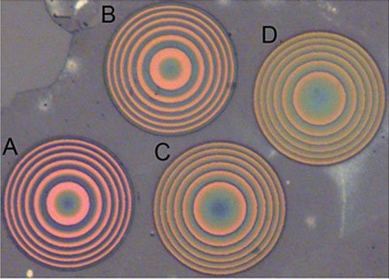
They tried the metalens’ viability by utilizing it to catch diverse test pictures, including of the Mona Lisa and a square letter W. The group likewise exhibited how extending the metalens could tune the central length of the lens.
Co-author Jiajiu Zheng, a doctoral student in electrical and computer engineering said, “We had to start by figuring out what type of design would yield the best performance given the incomplete phase.”
Majumdar said, “These results open up an entirely new platform for studying the properties of 2D materials, as well as constructing fully functional nanophotonic devices made entirely from these materials. Additionally, these materials can be easily transferred on any substrate, including flexible materials, paving a way towards flexible photonics.”
The study is published in the journal Nano Letters.