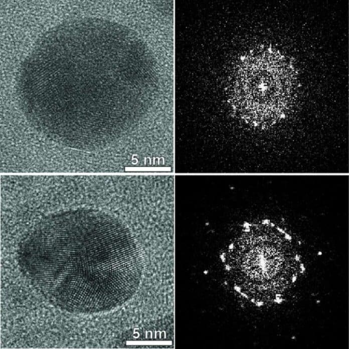
Researchers have been using advanced methods to learn how fluids interact with surfaces. They use tiny silicon nitride chips in high-tech electron microscopes as small-scale containers for their experiments. However, progress in this field has been hindered because the material around these chips scatters a lot of background noise.
This interference significantly reduces the quality of the microscope’s performance, especially when studying gases. The material used to seal the container creates a lot of interference, making it difficult to see things clearly and limiting the study’s accuracy.
Researchers at Northwestern University have devised a new way to study gas molecules in real-time. They were inspired by the honeycomb structures in nature and used this inspiration to create a fragile ceramic membrane to encase the gas sample during analysis.
This method helps understand the characteristics of gas atoms based on their unique bonds and improves the imaging of solid nanostructures when used in high-vacuum transmission electron microscopes. These microscopes are versatile tools that can be employed in various settings, from national laboratories conducting fundamental research to start-ups developing practical applications.
The silicon nitride microchip, designed by the Northwestern materials science team, reduces background scattering, which occurs when electrons deviate from their original path as they pass through a sample. This improvement enhances image resolution and contrast during the analysis.
The newly developed membrane is so thin that electrons can pass through the nanoreactor without distraction.
Materials scientist Vinayak Dravid said, “We anchored an ultra-thin silicon nitride film on our honeycomb framework, giving us a cell with membranes on either side.”
The before-and-after images displaying the reactions were striking.
Dravid said, “The thickness of the conventional membranes tends to be very large to maintain the mechanical integrity under the extremely high vacuum the microscope creates. Imagine I had to have very thick glasses that absorb a lot of light and, as a result, I don’t see much. The images we produced with our invention look almost like unfogging the glasses.”
Dravid likened the impact of their method to the transformation brought about by the James Webb Space Telescope, which revealed previously unseen celestial bodies. The innovative membrane developed by the research team enabled a level of spectroscopic analysis that could discern details down to a few gas atoms. This is particularly significant in distinguishing between molecules like carbon dioxide (CO2) and carbon monoxide (CO), which appear similar but play crucial roles in emerging clean energy technologies.
Spectroscopy allows scientists to observe how electrons interact with the atoms they study, revealing unique fingerprints regarding energy absorption, reflection, or emission.
Analyzing changes over time, under different pressures and temperatures, and understanding how fluids interact with nanoparticles is crucial for advancing clean energy and battery technologies at the molecular level. This breakthrough enables a more detailed analysis of applied technologies, such as photovoltaics and catalytic energy systems at the nano- and electronic length scales.
Xiaobing Hu, co-corresponding author and a research associate professor within the materials science and engineering department, said, “The ultra-thin ceramic membrane can be applied to broader discipline, not only limited to electron microscopy. For example, better results are expected for light- or X-ray characterizations. And the strategy can be widely extended for diaphragms and mechanical components which require low thickness but high mechanical strength.”
“With the new technique, we can see resolutions down to around 1.02 angstroms, compared to about 2.36 angstroms in previous experiments. We’ve achieved the highest spatial resolution and spectral visibility recorded in their field to date.”
Researchers are now looking forward to using their platform technology to other problems, as encapsulation could apply to any microchip or optical-based technique.
Journal Reference:
- Koo, K., Li, Z., Liu, Y., Ribet, S. M., Fu, X., Jia, Y., Chen, X., Shekhawat, G., M. Smeets, P. J., Park, J., Yuk, J. M., Hu, X., & Dravid, V. P. (2024). Ultrathin silicon nitride microchip for in situ/operando microscopy with high spatial resolution and spectral visibility. Science Advances. DOI: 10.1126/sciadv.adj6417
