Current electronic devices store information in the form of electronic charges—however, spin-a uniquely quantum property of electrons, offers an alternative. The spin can be controlled using polarised light to store information. Spin-polarized electrons, or spins aligned in a particular direction, are produced when a polarised light beam interacts with electron spins within a semiconductor.
So far, only uniformly polarised light, i.e., light with a spatially uniform polarisation, has been exploited to control electron spins. However, the production of spatially structured electron spins depends on the presence of an additional spatial structure (variation) in the polarization. This presents new possibilities for information storage.
To this end, a group of researchers, led by Junior Associate Professor Jun Ishihara from and including Graduate Student Takachika Mori, Graduate Student (at the time of the research) Takuya Suzuki, and Professor Kensuke Miyajima from Tokyo University of Science (TUS), Japan, has now devised a method for generating such spatially structured electron spins using a structured light with spatially varying polarization profile.
Scientists successfully generated a structured light beam with spatially variant polarization and transferred its structure to electron spins confined within a semiconductor solid. Additionally, they simultaneously generated two spin waves with inverted phases using this beam. Their results have essential implications in optical communications and information storage.
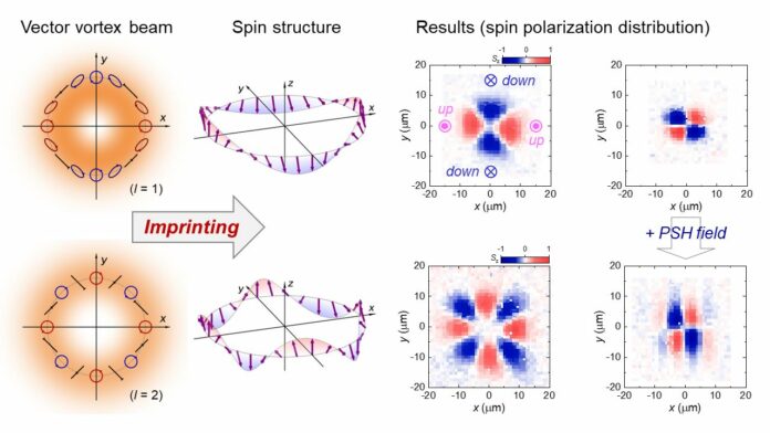
Junior Associate Professor Jun Ishihara said, “In this work, we generated a doughnut-shaped structured light-a vector optical vortex beam with an orbital angular momentum (OAM)-from a basic Gaussian beam using vortex half-wave plate and quarter-wave plate devices. We then used this beam to excite the electron spins confined within a gallium arsenide/aluminum gallium arsenide semiconductor quantum well. These spins, in turn, formed a helical spatial structure in a circle.”
Interestingly, while the beam with an OAM number equal to one produced a helix with two spin periods-spin up and spin down around the circle, an OAM number of two resulted in a helix with four such alterations. These observations indicated that the spatial polarisation structure of the optical vortex, determined by the OAM, was transferred to the electron spins inside the semiconductor.
In addition, increasing the OAM number was suggested to enable higher information storage capacity, characterized by a higher spin repetition rate around the circle.
Interestingly, while the beam with an OAM number equal to one produced a helix with two spin periods-spin up and spin down around the circle, an OAM number of two resulted in a helix with four such alterations. These observations indicated that the spatial polarisation structure of the optical vortex, determined by the OAM, was transferred to the electron spins inside the semiconductor. In addition, increasing the OAM number was suggested to enable higher information storage capacity, characterized by a higher spin repetition rate around the circle.
Dr. Ishihara said, “The conversion of the spatial polarization structure of light into a spatial structure of spin along with the generation of new spin spatial structures in combination with effective magnetic fields in solids are expected to lead to elemental technologies for higher-order quantum media conversion and information capacity enhancement using spin textures.”
Journal Reference:
- Jun Ishihara, Takachika Mori et al. Imprinting Spatial Helicity Structure of Vector Vortex Beam on Spin Texture in Semiconductors. Physical Review Letters. DOI: 10.1103/PhysRevLett.130.126701
