Understanding local dynamic charge processes is crucial for advancements in various fields, including microelectronics and energy storage. This requires the capability to track how charge carriers move over different distances and timescales and to comprehend how these processes interact with the natural variations in materials.
A team led by Marti Checa and Liam Collins from Oak Ridge National Laboratory has created an exciting way to understand how electric charges behave on a microscopic scale. Their work, published in Nature Communications, could help make batteries, solar panels, and other electronic devices work better and last longer.
In their study, the team talked about their new method that lets them see how electric charges move at the nanometer level, which is incredibly small but super fast. It’s like having a super-fast camera that can capture clear videos of a hummingbird’s wings flapping, whereas before, we could only see blurry pictures.
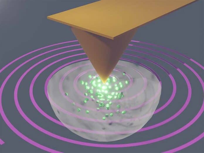
They used a scanning probe microscope and an intelligent control system that moves in a spiral pattern to scan things. They also used advanced computer programs to analyze the data. This new method lets them see how things work in detail, much better than before.
This new technique is a big deal because it helps scientists at the Center for Nanophase Materials Sciences at ORNL explore different materials and devices more efficiently.
Scientists noted, “This approach is shown to enable sub-second imaging of nanoscale charge dynamics, representing several orders of magnitude improvement over traditional Kelvin probe force microscopy imaging rates.”
“Together, these findings highlight the effectiveness and versatility of our method in understanding ionic charge carrier motion in microelectronics or nanoscale material systems.”
Journal Reference:
- Checa, M., Fuhr, A.S., Sun, C. et al. High-speed mapping of surface charge dynamics using sparse scanning Kelvin probe force microscopy. Nat Commun 14, 7196 (2023). DOI: 10.1038/s41467-023-42583-x
