
Scientists at MIT found a way to fabricate graphene with fewer wrinkles. This technique could efficiently produce wafer-scale, “single-domain” graphene i.e., single layers of graphene that are uniform in both atomic arrangement and electronic performance. Conventional graphene fabricating processes often generate wrinkles. Such graphene’s wrinkles can crash fast traveling of electrons that limits electrical performance.
In this new method, each electron flowed independently across each wafer, at similar speeds, even across previously wrinkled regions.
Jeehwan Kim, Assistant Professor in the departments of Mechanical Engineering and Materials Science at MIT said, “For graphene to play as the main semiconductor material for industry, it has to be single-domain so that if you make millions of devices on it, the performance of the devices is the same in any location. Now we can really produce single-domain graphene at the wafer scale.”
Usually, graphene production involves chemical vapor deposition or CVD. In CVD process, carbon atoms are deposited onto a crystalline substrate such as copper foil. The copper foil is then coated with carbon atoms and the entire thing is submerged into acid to etch copper. Hence, a graphene sheet is obtained.
The problem is that- this process create graphene’s wrinkles. In addition, the alignment of carbon atoms is not uniform across the graphene, creating a “polycrystalline” state in which graphene resembles an uneven, patchwork terrain, preventing electrons from flowing at uniform rates.
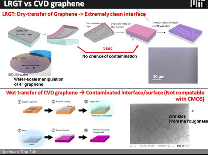
(CVD), in contrast, produces micron-scale wrinkles, with poor electrical performance.
In this new method, scientists used an automatically smooth surface of a silicon carbide wafer. They then used a thin sheet of nickel to peel off the topmost graphene from the silicon carbide wafer, in a process called layer-resolved graphene transfer.
But, before transferring the layer of graphene onto a silicon wafer, scientists oxidized the silicon and created a silicon dioxide layer that exhibits electrostatic charges. After depositing the graphene, in silicon dioxide, it effectively pulled graphene’s carbon atoms onto the wafer.
Kim said, “The CVD process creates wrinkles that are too high to be ironed out. For silicon carbide graphene, the wrinkles are just a few nanometers high, short enough to be flattened out.”
To test the single-crystalline graphene wafers, scientists designed tiny transistors on multiple sites on each wafer.
Kim said, “We measured electron mobility throughout the wafers, and their performance was comparable. What’s more, this mobility in ironed graphene is two times faster. So now we really have single-domain graphene, and its electrical quality is much higher than graphene-attached silicon carbide.”
“If you want to make any electronic device using graphene, you need to work with single-domain graphene. There’s still a long way to go to make an operational transistor out of graphene. But we can now show the community guidelines for how you can make single-crystalline, single-domain graphene.”