Lightweight semiconducting plastics are majorly been used in today’s mass market electronic displays such as those found in phones, tablets, and flat-screen televisions. The purpose of using these materials is to convert sunlight into electricity.
When this material absorbs light, they are in photo-excited states and need to move so that they can be “harvested” before they lose their energy. These excitations commonly just travel around 10 nanometres in plastic (or polymeric) semiconductors. Thus, scientists need to manufacture little structures designed at the nanoscale to boost the “harvest”.
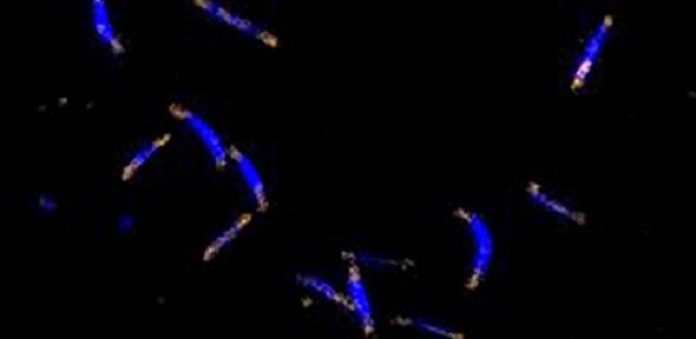
Now, scientists from the Universities of Cambridge and Bristol have demonstrated a technique to create plastic semiconductor nanostructures that absorb light and transport its energy 20 times further than has been previously observed. They have created highly ordered crystalline semiconducting structures using polymers.
Scientists believe that the technique could pave the to more flexible and more efficient solar cells and photodetectors.
Dr. Xu-Hui Jin and Dr. Michael Price of Cambridge’s Cavendish Laboratory measured the distance that the photo-excited states traveled, They were surprised to know that the technique reached distances of 200 nanometres – 20 times further than was previously possible. 200 nanometres is especially significant because it is greater than the thickness of material needed to completely absorb ambient light, making these polymers more suitable as “light harvesters” for solar cells and photodetectors.
Co-author Dr George Whittell from the University of Bristol said, “The gain in efficiency would actually be for two reasons: first, because the energetic particles travel further, they are easier to “harvest”, and second, we could now incorporate layers around 100 nanometres thick, which is the minimum thickness needed to absorb all the energy from light – the so-called optical absorption depth. Previously, in layers this thick, the particles were unable to travel far enough to reach the surfaces.”
Co-author Professor Sir Richard Friend from Cambridge’s Cavendish Laboratory said, “The distance that energy can be moved in these materials comes as a big surprise and points to the role of unexpected quantum coherent transport processes.”
Scientists are now planning to prepare structures thicker than those in the present investigation and more prominent than the optical absorption death, with a view to building model sun based cells in light of this innovation.
The study is originally reported in the journal Science.
