
Glass optical devices are hard to manufacture as they require a substantially higher molding temperature and extremely hard-to-machine carbide materials to make the mold. It is likewise hard to embellish micro and nanoscale optical components with micron-sized glass microstructures.
Nonetheless, with surging interest for powerful lenses of small size and high determination in cutting-edge optical systems, there has been mounting requirement for an optical glass to supplant optical polymers, which have much lower transmittance. Taking a DVD high-definition optical pickup lens, for instance, the element estimate is as small as 0.9 micron.
Traditional lithography strategies utilized for large-scale manufacturing result in high item costs, yet the lens created has much lower accuracy than those got from molding or embossing. Today, China has the most elevated yield of an optical lens in the world. However, because of innovative impediments for delivering high-end lenses, its aggregate market esteem is still lower than Europe and Japan.
Now, scientists at the Hong Kong Polytechnic University (PolyU) have developed a novel micro-embossing device for manufacturing precision glass lenses with high image quality. The lenses have the resolution required for state-of-the-art optical instruments and devices in varied fields including astronomy, national defense, medical scanning, and consumer products such as cameras and mobile phones.
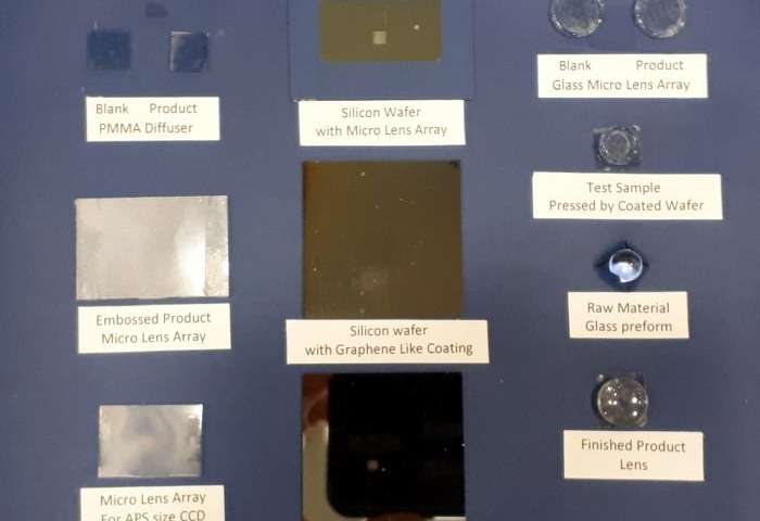
Scientists have received a novel molding design with graphene-like covering and self-created heating innovation to deliver the small-scale embellishing equipment to produce micron-level microstructural optical components in glass. Contrasted with regular massive infrared warming gadgets with high vitality utilization, the novel innovation is all the more eco-friendly and cost-efficient.
The use of a graphene-like coating can heat up the optical glass precisely and quickly with low energy consumption while reducing thermal expansion and deformation of the mold. The control and monitoring software can also provide instant online readings of the temperature to allow fine-tuning and adjustment of the process parameters, and thus shorten the cycle time.
Scientists noted, “Such novel features empower saving electric power by up to 60 times, contrasted with ordinary infrared machines, and reduce the assembling cost by 66%. Being an electrically conductive material with high wear attributes, graphene additionally enables smooth stripping of the glass workpiece from the shape after the emblazoning procedure. Moreover, a micron-scale example can be replicated on the glass substrate.”
The novel embossing equipment has wide applications in optoelectronics products, including cell phone micro-lenses, camera lenses, DVD pickup lenses, micro shuttle lenses, f-theta lenses for laser printers, projection television magnifiers, optical communication V Gutter substrates, micro-lens arrays (MLAs), and Fresnel lenses for collecting and tracking solar energy.