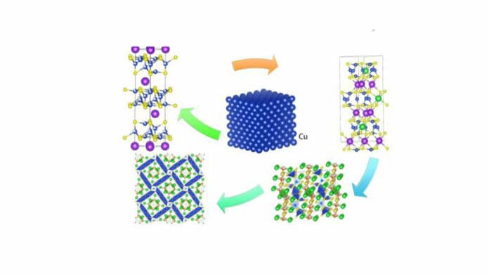
Numerous current technological advancements depend on the need for new material discoveries. However, comprehension of reactivity patterns is necessary for designing synthesis methods that lead to new and targeted solid-state materials. Synthesis science advancements are required to boost productivity and hasten the Discovery of new materials.
Scientists at the U.S. Department of Energy’s (DOE) Argonne National Laboratory, Northwestern University, and The University of Chicago have developed a new method for discovering and making new crystalline materials with two or more elements.
Xiuquan Zhou, a postdoc at Argonne and the first author of the paper, said, “Our invention method grew out of research on unconventional superconductors. These are solids with two or more elements, at least one of which is not a metal. And they cease to resist the passage of electricity at different temperatures—anywhere from colder than outer space to that in my office.”
The team’s invention process begins with a solution made from two components. One is a very efficient solvent. Any solids added to the solution dissolve in it and interact with it. The alternative is a less potent solvent. However, it is there to adjust how the reaction behaves when other elements are added to generate a new solid. The two components’ temperature and ratio are both adjusted during this tuning. Here, the temperature ranges from 750 to 1,300 degrees Fahrenheit, which is pretty high.
Mercouri Kanatzidis, a chemistry professor at Northwestern with a joint appointment at Argonne, said, “We are not concerned with making known materials better but with discovering materials no one knew about or theorists imagined even existed. With this method, we can avoid reaction pathways to known materials and follow new paths into the unknown and unpredicted.”
For testing, scientists applied their method to crystalline compounds made of three to five elements. Their discovery method yielded 30 previously unknown compounds. Ten of them have structures never seen before.
At the X-ray Science Division’s 17-BM-B of the Advanced Photon Source, a DOE Office of Science user facility at Argonne, and the UChicago ChemMatCARS beamline at 15-ID-D, the scientists have created single crystals of some of these novel compounds and described their structures.
17-BM-B beamline scientist Wenqian Xu said, “With beamline 17-BM-B of the APS, we were able to track the evolution of the structures for the different chemical phases that formed during the reaction process.”
Zhou said, “Traditionally, chemists have invented and made new materials relying only on knowledge of the starting ingredients and final product. The APS data allowed us to also take into account the intermediate products that form during a reaction.”
Given that practically any crystalline material may be processed using this technique, this is just the beginning of what is possible. It can also be used to create a variety of crystal formations. This comprises layers that are layered numerous times, a layer that is only one atom thick, and chains of unconnected molecules.
Such unusual structures have different properties and are key to developing next-generation materials applicable to not only superconductors but also microelectronics, batteries, magnets, and more.
Journal Reference:
- Xiuquan Zhou et al, Discovery of chalcogenides structures and compositions using mixed fluxes, Nature (2022). DOI: 10.1038/s41586-022-05307-7
