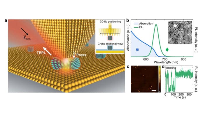
In a new study, scientists have presented a tip-induced control approach combined with tip-enhanced photoluminescence (TEPL) spectroscopy to engineer strain, bandgap, and the emission quantum yield of a single perovskite quantum dot. This approach allowed scientists to proficiently control the brightness and wavelength of quantum dots (QDs).
The study was conducted by an international team of scientists affiliated with UNIST.
Perovskite quantum dots are semiconducting nanocrystals. They are more tolerant to defects and have excellent photoluminescence quantum yields and high color purity.
Strain engineering of perovskite quantum dots (pQDs) enables widely tunable photonic device applications. However, manipulation at the single-emitter level has never been attempted.
This study discovered that hyperspectral TEPL imaging resolved single CsPbBrxI3–x pQDs with ~10 nm spatial resolution. Scientists then applied a plasmonic tip to a single pQD. This shifts bandgap up to ~62 meV with Purcell-enhanced PL increase as high as ~Lter105 for the strain-induced pQD.
Later, scientists modulated the tip-induced compressive strain of a single pQD. Doing so, they were able to achieve dynamical bandgap engineering reversibly. It also facilitates the quantum dot coupling for a pQD ensemble with ~0.8 GPa tip pressure at the nanoscale estimated theoretically.
Along with offering an in-depth understanding of the optical properties of metal halide perovskite pQDs and their coupling nature, this new approach provides a practical way to tune the mechanical and electronic properties at the single-pQD level.
Scientists noted, “This dynamical single-dot manipulation will enable the tunable nano-LEDs, realizing ultra-high-definition display with high efficiency. In addition, extremely high tip-induced local pressure will allow pressure-induced recrystallization and phase transition at the few-nanometer-length scale to further improve the grain quality and optical properties of 2D perovskite ensembles as a post-fabrication process.”
“Furthermore, the extrinsically modified physical properties of pQDs by the plasmonic cavity, e.g., reduced nonradiative recombination, modulation of carrier dynamics and PL lifetime, and enhanced radiative decay rate, can significantly improve the efficiency of perovskite photovoltaics.”
Journal reference:
- Hyeongwoo Lee, Ju Young Woo, Dae Young Park, et al., “Tip-Induced Strain Engineering of a Single Metal Halide Perovskite Quantum Dot,” ACS Nano, (2021). DOI: 10.1021/acsnano.1c02182
