Two-dimensional (2D) materials are promising candidates for future electronics. Although promising results on the wafer-scale synthesis of monolayer molybdenum disulfide (MoS2) have already been reported, the high-quality synthesis of 2D materials on wafers of 200 mm or larger, which are typically used in commercial silicon foundries, remains difficult.
To achieve this, MIT scientists have recently developed a cutting-edge technology that can successfully and quickly “grow” layers of 2D transition metal dichalcogenide (TMD) materials right on top of an entirely produced silicon chip, enabling denser integrations.
To prevent the chip from getting damaged, scientists also developed a low-temperature growth process that allows 2D semiconductor transistors to be directly integrated on top of standard silicon circuits.
According to scientists, their new technology could reduce the time it takes to grow these materials. It can grow a uniform layer of TMD material in less than an hour over 8-inch wafers.
Thanks to its high speed and uniformity, the technology allows scientists to successfully integrate a 2D material layer onto much larger surfaces than previously demonstrated. This makes their method better suited for commercial applications, where 8 inches or larger wafers are essential.
Jiadi Zhu, an electrical engineering and computer science graduate student, said, “Using 2D materials is a powerful way to increase the density of an integrated circuit. What we are doing is like constructing a multistory building. If you have only one floor, which is the conventional case, it won’t hold many people. But with more floors, the building will hold more people that can enable amazing new things. Thanks to the heterogeneous integration we are working on, we have silicon as the first floor, and then we can have many floors of 2D materials directly integrated on top.”
In this study, scientists mainly focused on molybdenum disulfide. This material is flexible, transparent, and exhibits powerful electronic and photonic properties that make it ideal for semiconductors. It comprises a one-atom layer of molybdenum sandwiched between two sulfide atoms.
Two organic chemical compounds contain molybdenum and sulfur atoms: Molybdenum hexacarbonyl and diethylene sulfur. Vaporizing and heating them inside a reaction chamber causes them to decompose into smaller molecules. Then they link up through chemical reactions to form chains of molybdenum disulfide on a surface.
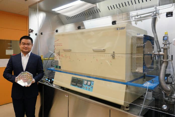
However, the decomposition of these compounds requires a maximum temperature of 550 degrees Celsius. On the other hand, silicon circuits would start degrading after surpassing 400 degrees. Hence, scientists came up with an alternative solution: They designed and built an entirely new furnace for the metal-organic chemical vapor deposition process.
The oven has two chambers: a front low-temperature area where the silicon wafer is inserted and a back high-temperature area. The furnace is pumped with precursors of vaporized molybdenum and sulfur. The temperature is controlled below 400 degrees Celsius in the low-temperature area, where the molybdenum remains. This temperature is hot enough to disintegrate the molybdenum precursor but not too hot to harm the silicon chip.
The sulfur precursor passes through and breaks down at the high-temperature area. The chemical reaction generates molybdenum disulfide on the surface of the wafer and then flows back into the low-temperature area.
A problem with this method is that silicon circuits frequently have an aluminum or copper top layer so the chip can be linked to a carrier or packaging before it is put onto a printed circuit board. But like some metals rust when exposed to oxygen, these metals become sulfurized when exposed to sulfur, which reduces their conductivity. To stop sulfurization, scientists first applied a very thin coating of passivation material on the chip’s surface. The passivation layer could then be opened later on to facilitate connections.
Additionally, they inserted the silicon wafer vertically, as opposed to horizontally, into the low-temperature area of the furnace. Because it is positioned vertically, neither end is too close to the area of high temperature, protecting the wafer from heat damage. Additionally, rather than flowing over a horizontal surface as they collide with the vertical chip, the molybdenum and sulfur gas molecules swirl as they hit the chip. The growth of molybdenum disulfide is enhanced by this circulation action, which also increases material homogeneity.
In addition to yielding a more uniform layer, their method was much faster than other MOCVD processes. They could grow a layer in less than an hour, while typically, the MOCVD growth process takes at least an entire day.
They demonstrated great material homogeneity and quality throughout an 8-inch silicon wafer using cutting-edge MIT.Nano facilities are crucial for commercial applications where larger wafers are required.
Zhu said, “By shortening the growth time, the process is much more efficient and could be more easily integrated into industrial fabrications. This is a silicon-compatible low-temperature process, which can be useful to push 2D materials further into the semiconductor industry.”
Journal Reference:
- Zhu, J., Park, JH., Vitale, S.A. et al. Low-thermal-budget synthesis of monolayer molybdenum disulfide for silicon back-end-of-line integration on a 200 mm platform. Nat. Nanotechnol. (2023). DOI: 10.1038/s41565-023-01375-6
